
Goal
To add machine code instructions to the computer. We need to modify the current hardware to allow us to fetch instructions, and then map to the correct microcode routine to execute that instruction. To do this we need to:
- A OPCODE mapper. This is logic to take an opcode, and causes the microsequencer to jump to the microcode for this instruction.
- Add a bit to the microcontrol word called “Fetch”. This tells the computer to read the next instruction pointed to by the PC and send the OPCODE bits to the microsequencer for decoding.
- Add a PC. Rather add a new register we can simple re-purpose the B register as a PC. This gives the added benefit that we can manipulated the PC in the same way the other registers are manipulated.
- Clear the PC on reset. We do this by asynchronous clear to our register.
- Allow the memory address to come from either the MAR or PC. The address with come from the MAR unless a fetch is happening.
- Store the N and Z bits in flop-flops. We need to do this so that a branch instruction can access the previous instruction’s results.
- Add a way to get only the lower 8 bits of an instruction, which is often either an address or data. We will do this by adding an alternate path for putting memory output on the A bus.
- Finally we need to add the microcode We will only start this in this lab, and continue it in future labs.
Note: The “C” register from the prvious lab has been renamed “B” for a bit more consistancy.
Resources
Introduction
This is a pivotal lab in the course of building your complete computer. It is very important that you complete it this week in order to move on to the next lab. It is fairly complex, but I will be spending time in class talking about it to get things going. We will first modify the computer to allow us to fetch instructions from memory, and map those instructions to a place in the microcode where it can be executed.
The goal of the system is to implement the following instructions.
Instructions
These are the ISA level instructions we will be supporting.
Where add or n below is the value of bits [0-7] in the nstruction, and the opcode is in bits [8-11].
| Opcode | Mnemonic | Meaning | Description |
|---|---|---|---|
| 0 | AND add | ACC <- ACC ^ mem( add) | AND memory – AND memory location “add” with the ACC |
| 1 | ADD add | ACC <- ACC + mem( add ) | Add memory – add memory location “add” to ACC |
| 2 | LOAD add | ACC <- mem( add ) | Load memory – load memory location “add” to ACC |
| 3 | STORE add | Mem( add ) <- ACC | Store memory – Store the ACC into the memory location “add” |
| 4 | SUB add | ACC <- ACC – mem( add) | Subtract memory – subtract memory location “add” from the ACC |
| 5 | MUL add | ACC <-ACC * mem(add) | Multiply the ACC by a memory location |
| 6 | DIV add | ACC <- ACC/mem(add), B <-remainder | Divide instruction, uses B for remainder |
| 7 | BR add | Branch to add | Branch to address add |
| 8 | BEQ add | Branch to add if Z=1 | Branch to address add if the result of the last computation was 0 |
| 9 | BLT add | Branch to add if N=1 | Branch to address add if the result of the last computation was negative |
| F00 | CLRA | Clear ACC | Clear Acc |
| F01 | NOT | Not ACC | Not the ACC |
| F02 | NEG | Negate ACC | Negate the ACC |
| F03 | INC | ACC = ACC + 1 | Increment the ACC |
| F04 | DEC | ACC = ACC – 1 | Decrement the ACC |
| F05 | SWAP | ACC <=> B | Swap the ACC with the B register |
| F0E | NOP | Do Nothing | Do nothing |
| F0F | HALT | Stop execution | halt computer |
Instruction Format
These instructions are in two formats.
Steps
Step 1 – Build an op-code mapper
An opcode mapper takes each op-code and maps it to a place in ucode where the instructions to implement that instruction are contained. There are actually two type of instructions:
- What we need to do is to map these instructions to a place in memory. What we can do with group 1 above is simply form a microcode address as the opcode followed by three 0’s. If we also set bit 7 to zero, we end up with something we see with Type one instructions below. This means that the each instruction will map microcode memory location opcode*8. This will give up to 8 micro instructions for each ISA instruction.
For type 2 instructions we will set bit seven to 1, and use bits 0-3 from the instruction as bits 3-6, just as we did in type 1 with the opcode. This will map the instructions 8 words apart starting from microcode memory address 0x80.
This we need two address mapping rules.
One exception to the rule – the ADDI instruction. Instead of mapping to zero, it will map to microcode memory location 1! Why? Because we one to store the fetch instruction in memory location 0. This will greatly reduce the complexity of the computer (as you will see).
Can you make a map of what the microcode memory will look like?
Type 1 Instructions
| Opcode | Hex | Mnemonic | Meaning | Address |
|---|---|---|---|---|
| 0000xxxxxxxx | 0xx | AND add | ACC <- ACC ^ mem( add) | 0x01 |
| 0001aaaaaaaa | 1aa | ADD add | ACC <- ACC + mem( add ) | 0x08 |
| 0010aaaaaaaa | 2aa | LOAD add | ACC <- mem( add ) | 0x10 |
| 0011aaaaaaaa | 3aa | STORE add | Mem( add ) <- ACC | 0x18 |
| 0100dddddddd | 4nn | SUB add | ACC <- ACC – mem( add) | 0x20 |
| 0101aaaaaaaa | 5aa | MUL add | ACC <-ACC * mem(add) | 0x28 |
| 0110aaaaaaaa | 6aa | DIV add | ACC <- ACC/mem(add), B <-remainder | 0030 |
| 0111dddddddd | 7dd | BR add | Branch to Address | 0x38 |
| 1000aaaaaaaa | 8aa | BEQ add | Branch to Address if Z=1 | 0x40 |
| 1001aaaaaaaa | 9aa | BLT add | Branch to Address if N=1 | 0x48 |
| 1010aaaaaaaa | Aaa | ??? | Future Expansion | 0x50 |
| 1011xxxxxxxxx | Bxx | ??? | Future Expansion | 0x58 |
| 1100xxxxxxxxx | Cxx | ??? | Future Expansion | 0x60 |
| 1101xxxxxxxxx | Dxx | ??? | Future Expansion | 0x68 |
| 1110xxxxxxxxx | Ex | ??? | Future Expansion | 0x70 |
| 1111xxxxiiii | Fxi | see below | Zero Op Instructions | 0x80+i*8 |
Type 2
These instructions use bits [0-4] to determine one of 16 instructions. These instructions map to microcode memory address 256+8*[0-3].
| Opcode | Hex | Mnemonic | Meaning | Address |
|---|---|---|---|---|
| 111100000000 | F00 | CLR | Clear ACC | 0x80 |
| 111100000001 | F01 | NOT | Not ACC | 0x88 |
| 111100000010 | F02 | NEG | Negate ACC | 0x90 |
| 111100000011 | F03 | INC | ACC = ACC + 1 | 0x98 |
| 111100000100 | F04 | DEC | ACC = ACC – 1 | 0xA0 |
| 111100000101 | F05 | SWAP | ACC <=> B | 0xA8 |
| 111100000101 | F06 | ??? | Future Expansion | 0xB0 |
| 111100000101 | F07 | ??? | Future Expansion | 0xB8 |
| 111100000101 | F08 | ??? | Future Expansion | 0xC0 |
| 111100000101 | F09 | ??? | Future Expansion | 0xC8 |
| 111100000101 | F0A | ??? | Future Expansion | 0xD0 |
| 111100000101 | F0B | ??? | Future Expansion | 0xD8 |
| 111100000101 | F0C | ??? | Future Expansion | 0xE0 |
| 111100000101 | F0D | ??? | Future Expansion | 0xE8 |
| 111100000110 | F0E | NOP | Do Nothing | 0xF0 |
| 111100000111 | F0F | HALT | Stop execution | 0xF8 |
ISA Instruction Mapper
Below is a device to map the 12 bit instrution code to the microcode address as defined above.
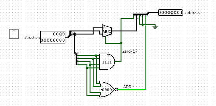
Note:
- The muxiplexor routes either the top four bits (8-11) to the output the bottom for bits (0-3).
- The output of the multipler is sent to bits (3-6) of the microcode address.
- If the opcode is F (1111), bits (0-3) are send to the microcode address (because it’s a type 2 instruction) otherwise bits (8-11) are sent.
- In the case where the opcode is 0 (0000) (ADDI), then set to low bit (0) to 1 so that we avoid using memory address 0.
To Do
- Build the circuit above.
- Test it out for several instructions of each type (1 and 2)
- Make sure it works for ADDI (opcode 0)
- Paste a picture of it with a type 1 and a type 2 instruction coming in.
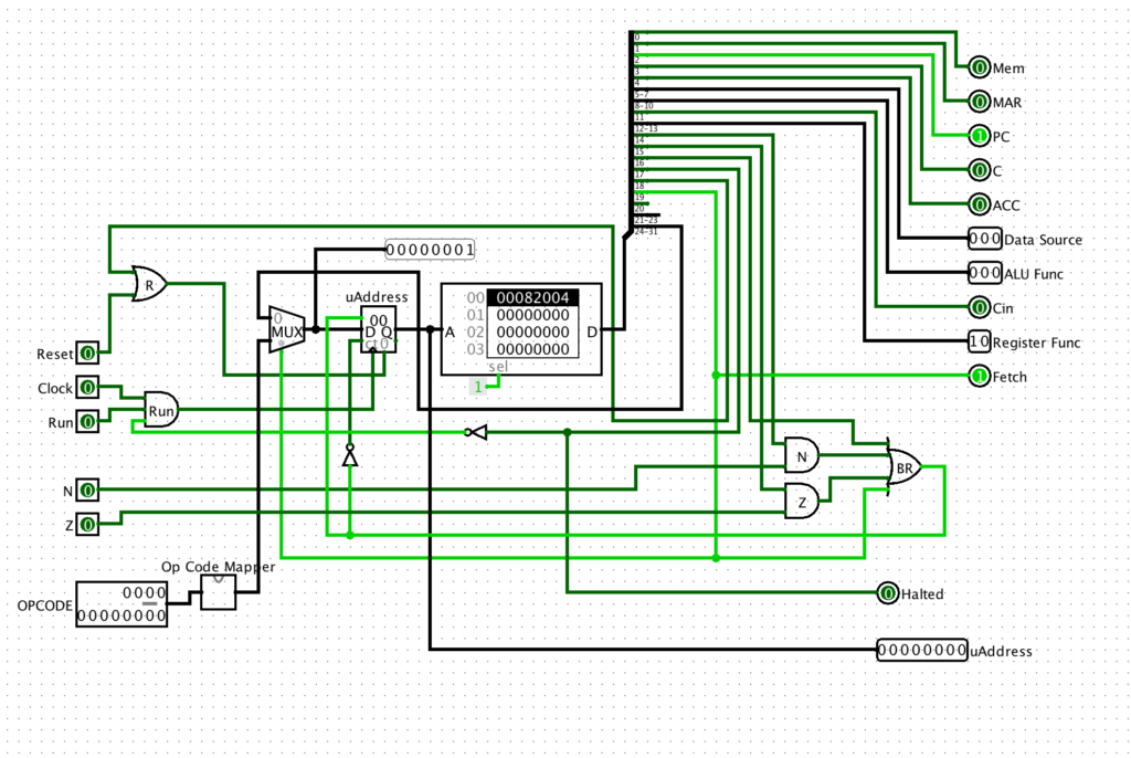
Step 2 – Update the microcode sequencer.
The sequencer from the previous lab can now be extended to include the instruction mapper. As you recall, the previous sequencer either incremented and used the micro-PC for the next address, or used the addess embedded in the microinstruction to determine the next microcode instruciton address. We now have a third option for the next address, the output of the instruction mapper.
What we need to do is to modify the sequencer to integrate the mapper in to also allow the instruction to determine the next mircocode address. This is done below by adding a muliplexer to select between the microcode address field and the instruction mapper. See the diagram below for the implementation. (I have added a probe to the multiplexer output to help with understanding and debugging).
To Do
- Modify your sequencer to use the mapper.
- Test it out. First make sure the new mapper works in place by adding a “Fetch” micro-instruction (0x80000) to the ROM at location 0, and placing several different OPCODE inputs. See if the sequencer jumps to the right next address. Take a screen shot of at least one successful mapping operation.
- Make sure the mapper still works for the other cases, e.g. for normal stepping though memory one instruction at a time, and for both conditional and unconditional branches.
Step 3 – Add and test new sequencer to main computer.
The circuit below shows the sequencer finally added to the main computer. This is it. If you get this together you finally have a fully capable system, waiting for it’s instruction set to be built in the microcode! Build the system as seen here. There are a few IMPORTANT changes:
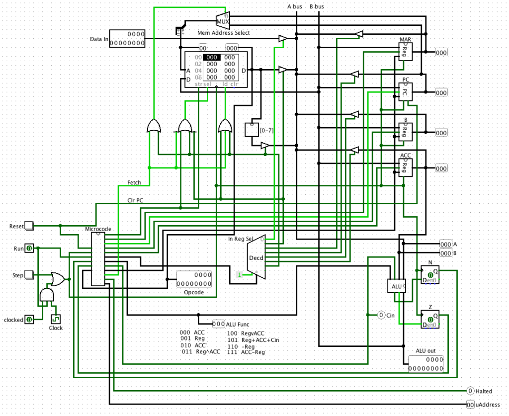
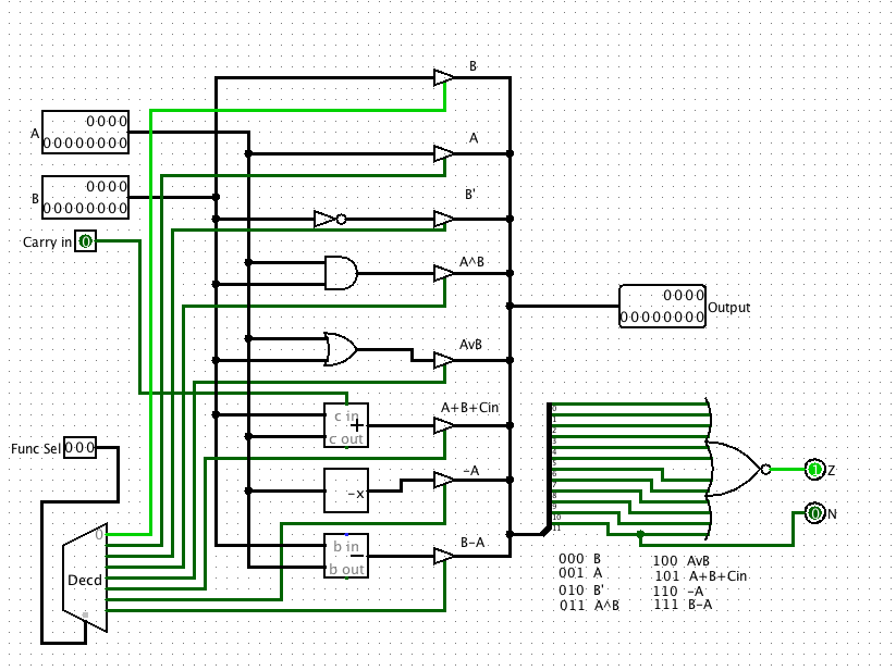
- Notice the D flip flops connected to the ALU. These are very important. Now that we we are integrating the full system we need to be able to have one machine instruction (that is a branch) use the conditions of the previous instruction to make it’s branch decision. For axample, we might load a value into the ACC, and then want to branch if the value is a zero. At the instruction level, one we have moved the data, and are now on to the next instruction, the very act of fetching the next instruction will change the output of the ALU based on this fetch. So we need to be able to “remember” the status one clock cycle back in time.
The solution is the flip flop. At the end of every CPU cycle, the current output of the Z and N bits are locked into the flip flops, then on the NEXT cycle, the Z and N bits represent the previous state of these bits. So any decision needs to be made exactly one clock cycle after the ALU computes a result. - Another ALU change (sorry). In order for the Z and N bits to be useful, they need to read meaningful data from the output of the ALU. Basically this designe will sense the output of the ALU at the end of each operation, and these values will be available for the next clock cycle. But what about operations that don’t involve the ALU (like branch, fetch, NOP). After some thought, I realized that the BEST default behavior is to have the ACC pass through the ALU if nothing else was done with the ALU. So I rearranged the ALU to have the B input (the ALU) be the default (e.g. when the function bits are 000). BELOW is a modified ALU, and an actual download of it to speed things up:
- As mentioned above, old C register is renames B, just to make more sense (we now have an ACC and B register.)
- We need a PC, that is a way to keep track of the instructions as we fetch them. We can take the B register and turn it into a PC. This requires that the PC now also (like the MAR) can act as a memory address as well. We need to a multiplexer to select between the MAR and the new PC as a address input to the memory address bits.
- What we need is a new microinstruction bit to select between the MAR and the PC. We call this the “Fetch” bit. We select the “Fetch” micro operation when we wish to use the PC as the address of the next instruction. Thus this Fetch bit (bit 19, or 0x80000) is used as the input to the new multiplexer.
- The PC is now a special register. When we turn the computer on, we need to start things up correctly, that is start executing code from some known location to “boot” the computer. This will be memory location zero. Thus we need to clear the PC every time we hit the reset button. So a new type of register has been created with a clear line connected to the reset: (See below)
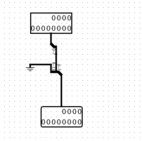
- When we fetch an instruction we now have to have a way for grabbing and using the bottom 8-bits of an instruction as an address. The easiest way to achieve this is to use one of the unused outputs on the source decoder to select an alternative output from memory. I have used the 7th pin on the decoder (6, or 110) to select the output from memory that has been routed through a simple device that masks off the top 4 bits, leaving only the lower 8. Below is the insides of this device:
- Before there would only two ways we accessed memory, either to write (assert str and sel inputs) or read(assert sel and ld inputs). Now there are four ways:
- Write to memory (as before)
- Standard read from memory (as before)
- When we fetch from memory (a read also)
- When we read the lower 8-bits) (also a read)
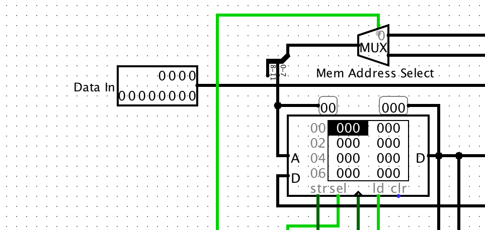
Thus the three or gates below the memory are used to correctly enable the memory inputs for these four conditions. Study them carefully, and then add them
- I have added a few probes to the system to show the system state. This is very useful in debugging you system.
- I have added an actual clock. A clock outputs a series of pulses, and can be useful when actually running a program. The “clocked” selector lets you decide between either a manually stepped system, and clocked system. The clock must be enabled in the top “Simulate” menu, and the tick frequency can be changed there.
To Do
- Complete the computer as seen above.
- Test the reset operation. The PC should clear on reset.
- Test the sequencer with the mapper in place. Put a fetch (0x80000) in memory location 0. Put an instruction in memory. Try an “ADD” (see the instructions in the table in he next section), that is put 105 in location zero in main memory (ADD’s memory location 5 to ACC). Step through the program an verify that as soon as you start, the microcode jumps to the microinstruction in location 0x08 in the ROM. (This is where we will be writing the microcode for the add instruction). Make sure also that the sequencer still increments when not fetching.
- Come up with a strategy for testing the new hardware to get the lower 8 bits of the memory. Describe your test, and show a picture of the results.
- Test the new clock. Explain how you tested it, and how it worked.
Step 4 – Start micro-coding
Below are the current tables for all the features available for the microcoded processor. Review them carefully.
Microcode instructions
Below is the definition for the micro-program control words:
| Branch Address | Unused | Fetch | Reset | Halt | Uncond Branch | Z | code N | Reg Func | Cin | ALU Func | Data Source | ACC | B | PC | MAR | Mem |
|---|---|---|---|---|---|---|---|---|---|---|---|---|---|---|---|---|
| 31-24 | 23-20 | 19 | 18 | 17 | 16 | 15 | 14 | 12-13 | 11 | 8-10 | 5-7 | 4 | 3 | 2 | 1 | 0 |
| 0xFF000000 | 0x80000 | 0x40000 | 0x20000 | 0x10000 | 0x8000 | 0x4000 | 0x3000 | 0x800 | 0x700 | 0xE0 | 0x10 | 0x8 | 0x4 | 0x2 | 0x1 |
The bit fields are defined as follows:
ALU Functions
| Bits | Operation |
|---|---|
| 000 | ACC |
| 001 | Reg |
| 010 | ACC’ |
| 011 | Reg ^ ACC |
| 100 | Reg V ACC |
| 101 | Reg + ACC + Cin |
| 110 | -Reg |
| 111 | ACC-Reg |
Data Source
| Bits | Source |
|---|---|
| 000 | Input |
| 001 | Memory |
| 010 | MAR |
| 011 | PC |
| 100 | B |
| 101 | ACC |
| 110 | Memory[0-7] |
Reg Func
| Bits | Func |
|---|---|
| 00 | Load |
| 01 | Clear |
| 10 | Increment |
| 11 | Decrement |
Now let’s consider a very simple test. We will add the microcode for the ADD instruction, and the CLR (clear ACC) instructions. We can use the following advanced microprogramming tool to create the microcode: Microcode generator version 4.
We need to start microprogramming the system. We set location zero to a fetch instruction. The add instruction will map to memory location 0x8, so we put the code for it there. And the clear instruction will map to location 0x80, so we put the code for that there:
| Instruction | Address | Microcode | Operation |
|---|---|---|---|
| Fetch | 0 | 00080000 | Fetch and dispatch instruction |
| 1 | |||
| ADD | 8 | 000001c2 | MAR ⇐ Mem(PC)[0-7] |
| 9 | 00000530 | ACC ⇐ Memory+ACC+Cin | |
| A | 00002004 | (PC) ++ | |
| B | 00080000 | Fetch | |
| C | |||
| CLRA | 80 | 00001010 | (ACC) ⇐ 0 |
| 81 | 00002004 | (PC) ++ | |
| 82 | 00080000 | Fetch | |
| 83 | |||
| Halt | F8 | 00020000 | Halt |
| F9 |
To Do
- Use the program online to generate the code above. Use the save button to save the microcode. Load the microcode into the ROM of the micro-sequencer.
- Create a program:
    CLRA
    ADD 5
    ADD 6
    Halt
Put this in main memory as:
| Address | Code | Assembler Code |
|---|---|---|
| 0 | F00 | Clear ACC |
| 1 | 105 | Add mem(5) to the ACC |
| 2 | 106 | Add mem(6) to the ACC |
| 3 | F0F | Halt |
Put a number in mem(5) and mem(6) to add. Try it out.
To Do
- Get the above program to work
- Show a shot of the final result.
- Writeup: What did you learn? What challenged you? What overall did you think of the lab?
- If your find a spelling or grammar error, and are the first to report you can get 1% extra credit.
- If you find, and propose a fix that works, to a technical issue, your will get 5% extra credit.